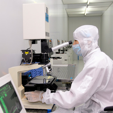
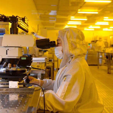
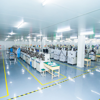
NewSemi founded in 2003, is a professional integrated circuit wafer design, R&D, production and semiconductor device packaging and testing manufacturer,Newsemi Semiconductor has a professional product research and development team and an advanced packaging and testing manufacturing factory. Schottky, MOS, IGBT, and Power wafers are all from well-known semiconductor listed companies at home and abroad.
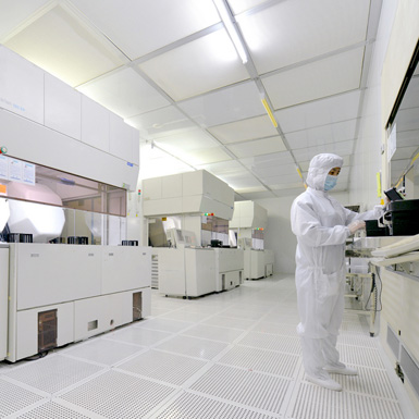
Over the years, NewSemi has accumulated rich experience in the industry, and a number of international advanced packaging and testing production lines have been put into production successively.The main packaging and testing production lines are SMA, SMAF, SMB, SMBF, SMC, SMCF, SOD, SOT, TO, SOP, DIP, DFN and so on. Packable and testable products include: Rectifier Diode, Switching Diode, Zener Diode, Schottky diode, TVS, ESD, Triode, Darlington, Mosfet, three-terminal voltage regulator, silicon controlled rectifier,lightning protection tube, discharge tube, integrated circuit, etc.
NewSemi is committed to the production and sales of wafers and semiconductor discrete devices, and can also provide semiconductor solution design, product customization and other related supporting services. Our company has passed ISO9001, ISO14001, QC080000, OHSAS18000, IATF16949 certifications.NewSemi product application market including:smart phones, computers, tablet computers, computer peripherals, headphones, set-top boxes, etc, and is widely used in communication, security, industry, automotive electronics, power supply, household appliances, smart homes, smart wear, new energy, photovoltaic, medical equipment, military industry and aerospace products.
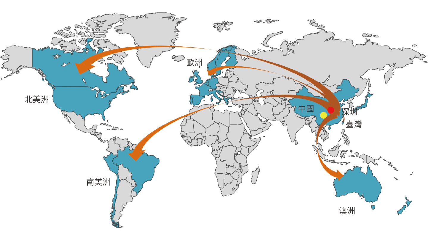
In order to serve our global customers better and provide customers with convenient technology and sales services, the company has set up laboratories and sales outlets in major cities around the world, as well as bonded warehouses and overseas warehouses to ensure rapid delivery of products.
-
2003
-
2006
-
2008
-
2012
-
2015
-
2016

Enterprise Vision
Committed to becoming the world's leading semiconductor brand

Enterprise mission
“Core with caftsmanship” casts quality, ”core with creation" wins the future, and provides customers with first-class products and solutions;

Enterprise values
Create value for customers, employees, society and shareholders.
